Top 10 Best Tips for Electronic Board Design Success?
In the rapidly evolving field of electronic board design, success hinges on a mix of creativity and precision. Renowned expert Dr. Emily Chang emphasizes, "A well-designed board isn’t just about functionality; it’s about envisioning the whole ecosystem." This perspective captures the essence of effective electronic board design.
Designers must navigate numerous challenges. Balancing aesthetics with practicality is a constant struggle. Effective thermal management, for example, often gets overlooked. Ignoring this aspect can lead to failures later in the product lifecycle. Moreover, while sophisticated tools are available, they can overwhelm beginners who may falter under pressure.
Attention to detail can make or break a project. Small mistakes in component placement can lead to significant performance issues. Designers often need to embrace setbacks as learning opportunities. Reflection on past experiences shapes future designs. In the quest for optimal electronic board design, flexibility and patience are essential.

Understanding the Basics of Electronic Board Design Principles
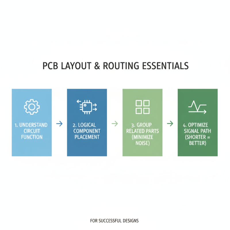
Electronic board design is a complex task that requires a solid understanding of fundamental principles. At its core, it involves creating a board that meets functional requirements while optimizing for space and cost. Designers must consider factors like signal integrity, thermal management, and power distribution. Each layer of the board serves a specific purpose, yet they must all work in harmony. It’s essential to visualize the flow of signals when sketching your layout.
Effective component placement can significantly affect performance. For instance, placing sensitive components away from noisy parts is crucial. Many new designers struggle with this. They often overlook the importance of grounding techniques. Proper grounding reduces interference. It fosters a clean signal path, but it takes practice. Reflection on past mistakes can lead to better designs. Learning from these errors is part of the journey.
Simulation tools can assist in validating your design before manufacturing. However, reliance on software alone can lead to complacency. Hands-on testing and prototyping are invaluable. Sometimes, the best lessons come from unexpected failures during real-world testing. Ultimately, balancing theoretical knowledge with practical experience will pave the way for successful electronic board design. Keep designing, keep learning, and embrace the challenges that come your way.
Top 10 Best Tips for Electronic Board Design Success
Identifying Key Components and Their Functions in Board Design
In board design, identifying key components is crucial. Each part serves a specific function and impacts overall performance. Power supplies regulate voltage. Capacitors filter noise, ensuring signal integrity. Resistors manage current flow. These components can cause issues if not chosen carefully.
Testing different configurations often reveals the most effective setup. It’s common to overlook minor details. For example, trace widths might appear sufficient but fail under load. Proper heat dissipation is another detail that can’t be ignored. Without it, your board could overheat and malfunction.
Components must also be compatible. This requires careful planning and research. Using suboptimal parts can lead to increased costs and time delays. Engineers often struggle to balance performance with budget constraints. Always be prepared to revise your designs. Expect unexpected challenges along the way. Each iteration can be a learning moment, refining your skills in board design.
Ensuring Signal Integrity and Minimizing Electromagnetic Interference
Ensuring signal integrity is crucial in electronic board design. Poor signal integrity can lead to data errors. A report by the IEEE noted that 37% of time in product development is spent troubleshooting signal issues. This highlights the importance of careful planning.
Tip: Utilize controlled impedance traces. This approach maintains consistent electrical characteristics over the length of the traces. It reduces reflections and ensures clean signal transmission. Moreover, minimize trace lengths where possible. Longer traces can pick up more noise, affecting performance.
Minimizing electromagnetic interference (EMI) is equally important. High-frequency designs are particularly sensitive to EMI. The IPC published data showing that over 40% of design failures are due to EMI issues. Implementing ground planes can help shield sensitive components. Additionally, route high-speed signals away from analog components to prevent interference.
Tip: Use twisted pairs for differential signals. This technique can cancel out EMI, promoting signal quality. Keep in mind that even with best practices, issues may still arise. Regular testing is essential. Analyzing prototypes for potential signal integrity and EMI problems can save time later in the design process.
Top 10 Best Tips for Electronic Board Design Success - Ensuring Signal Integrity and Minimizing Electromagnetic Interference
| Tip Number |
Tip Description |
Importance Level |
| 1 |
Use proper grounding techniques to reduce noise. |
High |
| 2 |
Maintain short signal paths to minimize delay. |
High |
| 3 |
Use differential signaling where applicable. |
Medium |
| 4 |
Incorporate proper decoupling capacitors. |
High |
| 5 |
Select appropriate PCB material to meet transmission needs. |
High |
| 6 |
Implement effective shielding techniques. |
Medium |
| 7 |
Minimize loop areas in your design to reduce EMI. |
High |
| 8 |
Use proper trace widths for all signal and power routes. |
Medium |
| 9 |
Plan power distribution carefully to ensure voltage stability. |
High |
| 10 |
Regularly simulate and test designs before final production. |
High |
Strategies for Prototyping and Testing Your Electronic Board Design
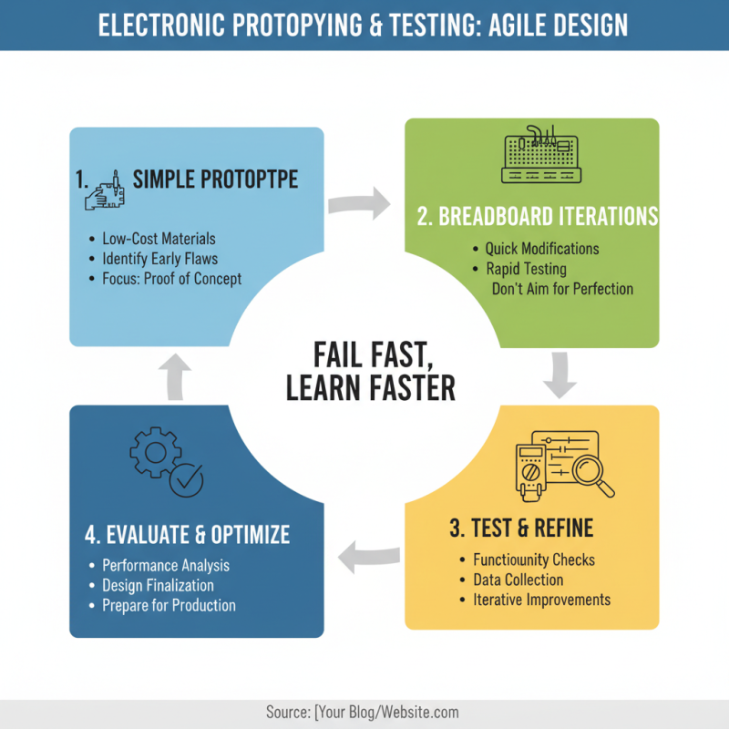
Prototyping and testing an electronic board design can be challenging. Start with a simple prototype. Use low-cost materials. This helps in identifying design flaws early. Breadboards are useful for quick iterations. They allow rapid modifications. Don’t aim for perfection at this stage. Instead, focus on proof of concept.
Testing is crucial. Conduct various tests to evaluate your design's functionality. Look for any inconsistencies. Sometimes, unexpected issues arise. For instance, check for signal integrity early on. Run thermal tests to ensure components do not overheat. Document all findings, including failures. This feedback loop is essential for refining your design.
Consider user feedback as well. Present prototypes to potential users. Observe their interactions. Their insights can guide improvements. Adjust based on their responses. It’s important to remain flexible. Expect some design aspects may not meet initial expectations. Reflect on these points for future iterations. Overall, the journey of refining your electronic board is continuous and iterative.