What is PCB and Assembly Process Explained for Beginners
In the ever-evolving world of electronics, the concepts of PCB and assembly are fundamental for both novices and seasoned professionals. Printed Circuit Boards (PCBs) serve as the backbone of electronic devices, enabling efficient connectivity and functionality. As expert Dr. Emily Chen, a leading authority in the field of electronics manufacturing, aptly stated, “Understanding the PCB and assembly process is crucial to mastering modern electronic design.” This assertion highlights the need for aspiring engineers and hobbyists to grasp the intricacies involved in creating these essential components.
The PCB and assembly process encompasses various steps, from design and fabrication to assembly and testing. Each phase plays a significant role in ensuring the final product meets the required standards of quality and performance. For beginners, delving into this topic can feel overwhelming; however, a clear understanding of each step is key to successfully developing reliable electronic devices. By breaking down the components of PCB and assembly, individuals can gain the confidence necessary to navigate this complex landscape and contribute to the innovative technology of tomorrow.
What is a PCB? Understanding the Basics
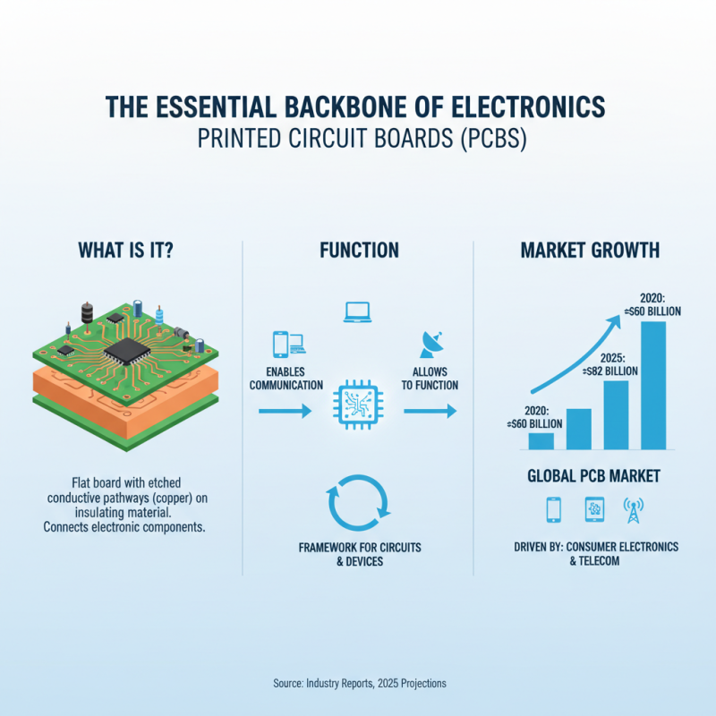
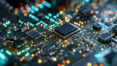
PCB, or Printed Circuit Board, serves as the backbone of almost all electronic devices. It is a flat board made of insulating material, which contains conductive pathways etched from copper sheets. These pathways connect various electronic components, allowing them to communicate and function together. According to industry reports, the global PCB market is expected to reach $82 billion by 2025, driven by the increasing demand for consumer electronics and telecommunications devices. Understanding PCBs is vital for anyone looking to delve into electronics, as they form the essential framework for circuits and devices.
When starting out in PCB design and manufacturing, it is essential to familiarize oneself with the dos and don’ts of the assembly process. Tips for beginners include ensuring the design layout optimizes space while maintaining signal integrity, and selecting the right materials for the board based on the intended application. Often, novice designers overlook the importance of thermal management in PCB design, which can lead to overheating and potential failures.
Moreover, staying updated with industry standards and technological advancements can significantly enhance your PCB design skills. Engaging in community forums and utilizing simulation software can provide valuable insights. The 2022 IPC Report highlighted that companies focusing on continuous innovation in PCB manufacturing tend to outperform their competitors, showcasing the importance of maintaining a robust design and assembly process.
Types of PCBs: A Beginner's Overview
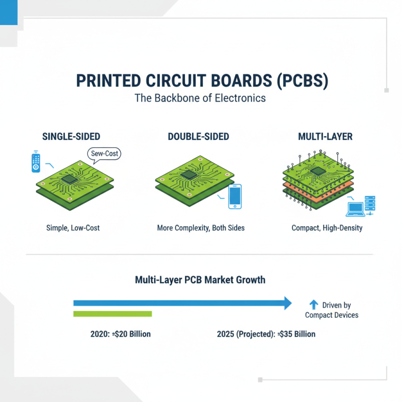
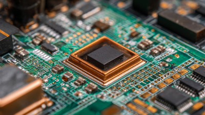
Printed Circuit Boards (PCBs) are integral components in electronic devices, serving as the backbone for electrical connections. Various types of PCBs cater to different applications and industries, providing essential functions based on specific design and manufacturing techniques. The most common types of PCBs include single-sided, double-sided, and multi-layered boards. According to industry reports, the multi-layer PCB market is expected to grow significantly, projected to reach approximately USD 35 billion by 2025, driven by advancements in electronics and the increasing demand for compact devices.
Single-sided PCBs are characterized by their simplicity, featuring electronic components mounted on one side with conductive pathways etched on the other. They are cost-effective and widely used in low-density designs. Double-sided PCBs allow for more complex circuitry, accommodating components on both sides and enabling higher functionality. In contrast, multi-layer PCBs, consisting of multiple laminated layers, are essential in high-performance applications such as smartphones and computers, where space and efficiency are crucial. As the technology evolves, the variety of PCB types continues to expand, supporting the rapid growth of industries ranging from consumer electronics to aerospace, underscoring their vital role in modern technology development.
The PCB Design Process: Step-by-Step Guide
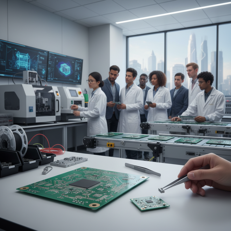
The PCB design process is an essential foundation for the development of electronic devices, encapsulating several critical steps. Initially, the journey begins with defining the specifications of the project, including size, placement of components, and functionality. According to a recent industry report from IPC, around 50% of PCB design failures can be traced back to improper specification definitions, underscoring the importance of this phase. Next, engineers usually move on to schematic capture, where the circuit diagram is created to ensure that all components are correctly connected. This step is crucial, as digital tools facilitate the detection of errors before the PCB layout is constructed.
Once the schematic is completed, designers input the data into PCB layout software, where they arrange components on the board and establish electrical connections. This phase requires a delicate balance between functionality and manufacturability, with studies showing that 70% of successful PCB designs adhere to strict design rules that optimize both performance and production efficiency. During the final verification stage, thorough simulations and checks are employed to validate the design against potential thermal, mechanical, and electrical issues.
**Tips:** To ensure a smooth PCB design process, it is advisable to collaborate early with manufacturing teams to align design capabilities with production processes. Additionally, utilizing automated design rule checks can significantly reduce the likelihood of errors during the layout phase, enhancing overall design integrity.
What is PCB and Assembly Process Explained for Beginners
| Step |
Description |
Duration |
Key Materials |
| 1 |
Designing the PCB layout using software tools |
2-5 days |
FR-4, Copper, Silkscreen |
| 2 |
Prototype fabrication of the PCB |
1-2 weeks |
Copper Laminates |
| 3 |
Component placement on the PCB |
1-3 days |
Resistors, Capacitors, ICs |
| 4 |
Soldering components to the PCB |
1-2 days |
Lead-free Solder, Solder Paste |
| 5 |
Testing the assembled PCB for functionality |
2-4 days |
Test Equipment, Probes |
Overview of PCB Assembly Techniques and Methods
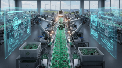
PCB assembly is a critical process in electronics manufacturing, involving the integration of various electronic components onto a printed circuit board (PCB). This process can be divided into several techniques and methods, each chosen based on the specific requirements of the project. Common assembly techniques include surface mount technology (SMT), through-hole technology (THT), and mixed technology, which combines both SMT and THT.
SMT is popular for its ability to place components directly onto the surface of the PCB, allowing for higher density and smaller designs. Conversely, THT involves inserting components through holes in the board, providing stronger mechanical connections that are beneficial for certain applications. Understanding these assembly methods helps beginners select the appropriate technique for their project, ensuring functionality and reliability.
Tips: When starting with PCB assembly, choose the method that best fits your design goals. Consider factors like component size, board dimensions, and the intended use of the device. Additionally, practice good soldering techniques to prevent short circuits or cold joints, which can compromise the integrity of your assembly. Finally, thoroughly test your assembled boards before deployment to identify any potential issues early on.
Common Applications of PCBs in Electronics and Technology
Printed Circuit Boards (PCBs) are integral to modern electronics, serving as the backbone of various applications across multiple sectors. According to a report by Market Research Future, the global PCB market is expected to reach approximately $82.25 billion by 2025, reflecting an annual growth rate of about 4.22%. This surge is driven by the escalating demand in consumer electronics, automotive systems, and telecommunications. In consumer electronics, PCBs are utilized in devices such as smartphones and laptops, where they facilitate connectivity and component interactions, ensuring efficient performance and compact design.
In addition to consumer electronics, PCBs are pivotal in the automotive industry. As vehicles become increasingly reliant on electronic systems for functionality—from navigation systems to advanced driver-assistance systems (ADAS)—PCBs play a crucial role. The automotive PCB market, valued at around $5.6 billion in 2021, is projected to grow at a staggering rate as electric and autonomous vehicles become more prevalent. Moreover, PCBs are essential in medical technologies, where they support critical functions in imaging equipment, diagnostic devices, and monitoring systems, emphasizing reliability and precision. This diversification highlights the central role of PCBs in advancing technologies across industries, driving innovation, and shaping the future of electronic applications.
Common Applications of PCBs in Electronics
This bar chart represents the common applications of Printed Circuit Boards (PCBs) in various sectors of electronics. Consumer electronics dominate the market, showcasing the widespread use of PCBs in everyday devices.