2025 Guide: How to Master Circuit Board Design for Optimal Performance
In the rapidly evolving field of electronics, mastering circuit board design is essential for anyone looking to achieve optimal performance in their products. According to Dr. Emily Chen, a leading expert in the industry, “Effective circuit board design not only enhances the functionality of electronic devices but also significantly improves their reliability and efficiency.” This statement encapsulates the importance of understanding the intricate details that govern the successful design of circuit boards.
As technology advances, the demand for more sophisticated and efficient circuit board design solutions rises. Designers are challenged to integrate complexity while ensuring reliability and performance. This guide aims to provide aspiring engineers and seasoned professionals with the knowledge and skills necessary to excel in circuit board design. By diving into the principles of design, layout, and testing, we will explore the crucial elements that contribute to creating high-quality circuit boards that meet the needs of modern applications. Embracing these methodologies is imperative for anyone seeking to lead in the circuit board design space.

Understanding the Basics of Circuit Board Design Principles
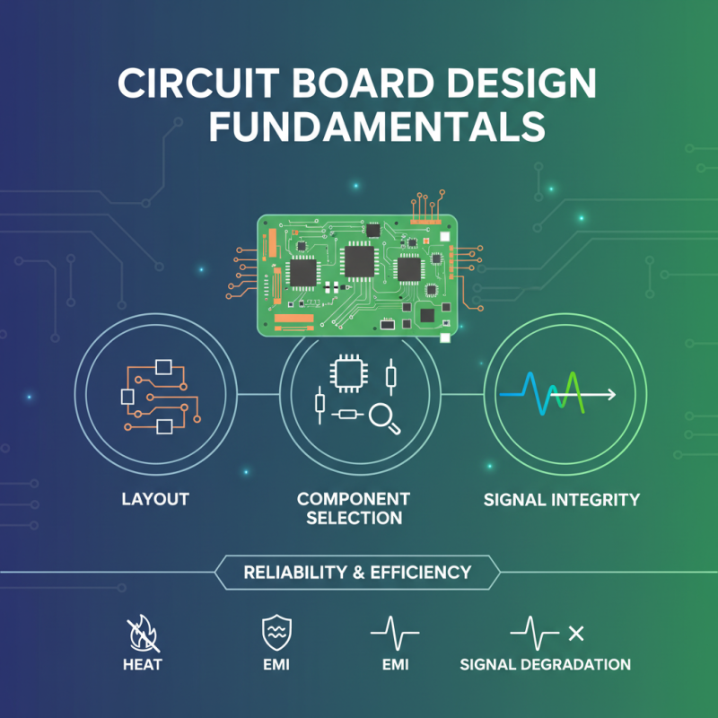
Circuit board design is a fundamental aspect of electronics, serving as the backbone for virtually all electronic devices. Understanding the basic principles of circuit board design is essential for creating reliable and efficient products. Several key factors influence the design process, including layout, component selection, and signal integrity. A well-designed circuit board not only enhances performance but also minimizes potential issues related to heat, electromagnetic interference, and signal degradation.
Tips for optimizing circuit board design include prioritizing component placement. Strategically arrange components to minimize trace length, which can reduce delay and interference. Moreover, consider the use of ground planes and proper routing techniques to improve signal integrity and decrease noise levels. Pay attention to thermal management by incorporating sufficient spacing and heat dissipation methods, ensuring that components operate within their safe temperature ranges.
Another crucial aspect is to keep design iterations in check. Always prototype and test early versions of your circuit board to identify flaws and optimize performance before mass production. Utilizing simulation software can help predict potential issues and streamline the design process. Remember, mastering these fundamental principles will significantly contribute to your success in circuit board design and ultimately lead to more effective and high-performing electronics.
Key Tools and Software for Effective Circuit Board Design
Effective circuit board design hinges on the right tools and software, which streamline the process and enhance the final product's performance. The essential software for circuit board design includes schematic capture tools that allow engineers to create and manipulate diagrams representing electronic circuits. These tools enable designers to efficiently organize components and connections, making it easier to troubleshoot and modify designs as necessary. Additionally, simulation tools are crucial, as they provide a virtual environment to test circuit functionality before manufacturing. This step can significantly reduce costs associated with physical prototypes.
Another key category of tools includes printed circuit board (PCB) layout software. These applications facilitate the arrangement of components on the board while considering factors like space, heat dissipation, and signal integrity. Integrated design environments that combine both schematic and layout functionalities can greatly improve efficiency. Moreover, features like automatic routing assist designers in creating optimal paths for electrical connections, further enhancing the board’s performance. Utilizing these tools not only accelerates the design process but also ensures a higher quality end product, paving the way for innovations in technology and electronic applications.
Designing for Optimal Electrical Performance and Signal Integrity
Achieving optimal electrical performance and signal integrity in circuit board design is critical for any electronic system.
The foundation of this process lies in understanding how electrical signals propagate through the circuit. One of the key principles is to
minimize electromagnetic interference (EMI) by carefully planning component placement and routing.
Ensure that sensitive components are positioned away from high-frequency traces, and utilize ground planes strategically to shield against unwanted noise.
This practice not only enhances signal clarity but also promotes better overall performance in the circuit.
Another essential aspect of ensuring signal integrity is employing proper trace width and spacing.
When designing traces, engineers need to account for the characteristics of the signals they will carry, considering factors such as current load,
impedance, and the effects of parasitic capacitance and inductance. As a rule of thumb, maintaining consistent trace width helps reduce reflections and
signal degradation.
Additionally, differential signaling can be leveraged to further bolster integrity, especially in high-speed applications,
as it inherently counters noise and improves data transmission accuracy.
By adhering to these fundamental principles, designers can create circuit boards that not only perform optimally but also stand the test of time
in a rapidly evolving technology landscape.
Best Practices for Component Placement and Routing Techniques
Effective component placement and routing are crucial elements in circuit board design that can significantly impact the overall performance of electronic devices. According to a report by IPC, a leading association for electronics manufacturers, proper component arrangement can reduce the size of the circuit board by up to 15%, which is essential in today's push for compact designs. Placing components closer together not only saves space but also minimizes the lengths of traces, which can help mitigate signal integrity issues and electromagnetic interference (EMI). Strategic placement can also enhance thermal management, as components generating heat can be positioned in a way that enables efficient heat dissipation.
Routing techniques play an equally important role in ensuring optimal performance. A study by Altium indicates that incorrect routing can lead to a 25% decrease in signal reliability, emphasizing the necessity of adhering to established design rules. Implementing differential pair routing for high-speed signals and ensuring adequate clearance between traces are fundamental practices that enhance signal integrity. Moreover, using tools like via stitching and ground planes aids in creating effective return paths for signals, reducing noise and improving performance. Ultimately, mastering these best practices in component placement and routing can lead to circuit boards that are not only high-performing but also meet the growing demands of smaller, faster, and more efficient electronic devices.
2025 Guide: How to Master Circuit Board Design for Optimal Performance
| Component Type |
Optimal Placement |
Recommended Routing Techniques |
Common Issues |
| Microcontroller |
Central location to minimize trace length |
Avoid sharp corners, use wide traces for power |
Signal interference and noise issues |
| Capacitor |
Close to the power pins |
Use vias to connect to ground plane |
Overheating and performance degradation |
| Resistor |
Near the related circuit components |
Keep traces short to reduce inductance |
Value drift due to temperature |
| Inductor |
Isolated area for magnetic flux |
Use differential pairs for sensitive signals |
Cross-talk and interference |
| Transistor |
Placement near power management areas |
Controlled impedance routing |
Thermal runaway risks |
Testing and Iterating Your Circuit Board Design for Improvement
Testing and iterating your circuit board design is crucial for achieving optimal performance, especially as the complexity of electronic devices increases. According to a report by the IPC Association Connecting Electronics Industries, about 60% of design failures can be attributed to inadequate testing processes. To address this, implementing a robust testing strategy is essential. Techniques such as Design for Test (DFT) and simulation software can identify potential issues before physical prototypes are created. By integrating DFT principles, designers can ensure that test points are accessible and that the circuitry facilitates efficient debugging, ultimately leading to a more reliable final product.
Moreover, iteration is an integral part of the design process. The Continuous Improvement methodology explained in the ASME’s guidelines emphasizes the importance of iterative testing and feedback loops. Each iteration should incorporate lessons learned from previous tests, allowing designers to refine their circuit boards based on real-world performance data. For example, thermal imaging and electrical testing can reveal hidden inefficiencies such as heat hotspots or signal integrity problems. In fact, data from a recent study indicated that companies that adopt a systematic approach to iteration experience a 50% reduction in development time, significantly accelerating time-to-market without compromising on quality. By prioritizing both testing and iteration, designers can enhance the performance and reliability of their circuit boards, resulting in better end products.
2025 Circuit Board Design Performance Metrics