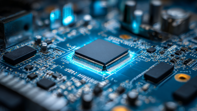
10 Essential Tips for Designing High-Quality Printed PCB Boards Efficiently
In the rapidly evolving landscape of electronics, the significance of designing high-quality printed PCB boards has never been greater. With the global printed circuit board market projected to reach over $85 billion by 2025, driven by the increasing demand for advanced electronic devices, efficient design methodologies are paramount. Industry reports indicate that innovations in PCB technology are not only enhancing performance but also enabling manufacturers to meet stringent deadlines without compromising on quality. For instance, studies reveal that businesses employing best practices in PCB design can reduce production costs by up to 30%, thereby gaining a competitive edge in the marketplace.
The emphasis on efficiency in designing printed PCB boards stems from the need to streamline production processes while ensuring high reliability and durability. As consumer electronics and automotive sectors drive the demand for more complex circuits, designers face the challenge of integrating functionality with manufacturability. To navigate this intricate balance, adopting proven strategies and modern design tools is essential. Addressing aspects such as layout optimization, material selection, and testing protocols can significantly enhance the performance and longevity of printed PCB boards. This article outlines ten essential tips for achieving these goals and staying ahead in the fast-paced world of electronics manufacturing.
Understanding PCB Layer Count and Its Impact on Performance and Cost
When designing printed circuit boards (PCBs), understanding the layer count is crucial as it directly influences both performance and manufacturing costs. A basic design may only require two layers, which is sufficient for simple circuits with minimal component density. However, as the complexity of the circuit increases, adding more layers can enhance signal integrity and power distribution. Multi-layer PCBs facilitate better routing of signals, allowing designers to incorporate more functionality within a smaller footprint, which is essential in modern electronic devices.
While increasing the layer count can improve performance, it also escalates production costs. Each additional layer not only adds to the material expense but also complicates the manufacturing process, requiring more advanced fabrication techniques. Consequently, it is essential to carefully evaluate the trade-offs between the desired performance attributes and the budget constraints. Designers should strike a balance by assessing the circuit's requirements, ensuring that the layer count aligns with both the operational needs and financial viability, ultimately leading to efficient, high-quality PCB designs.
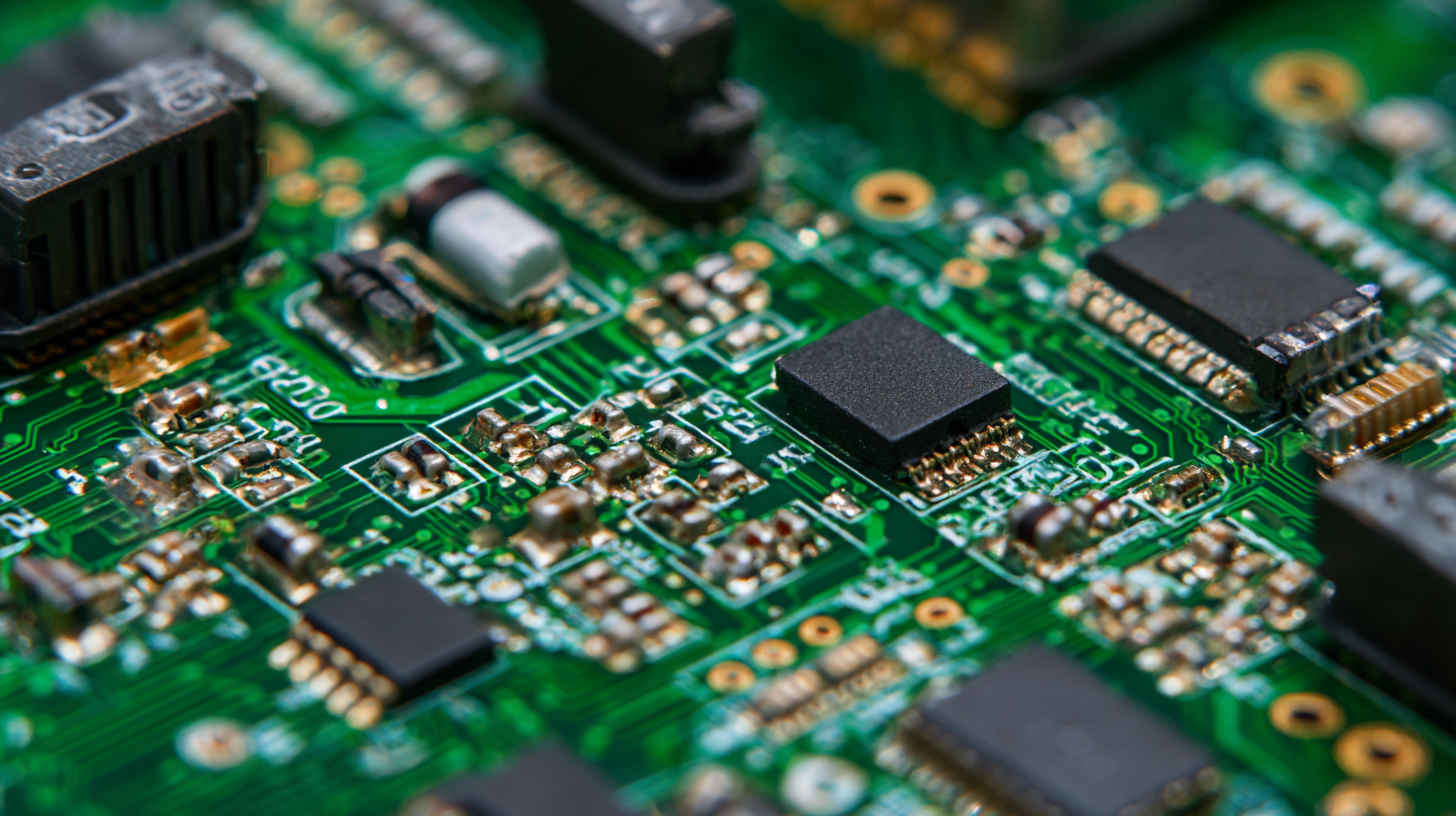
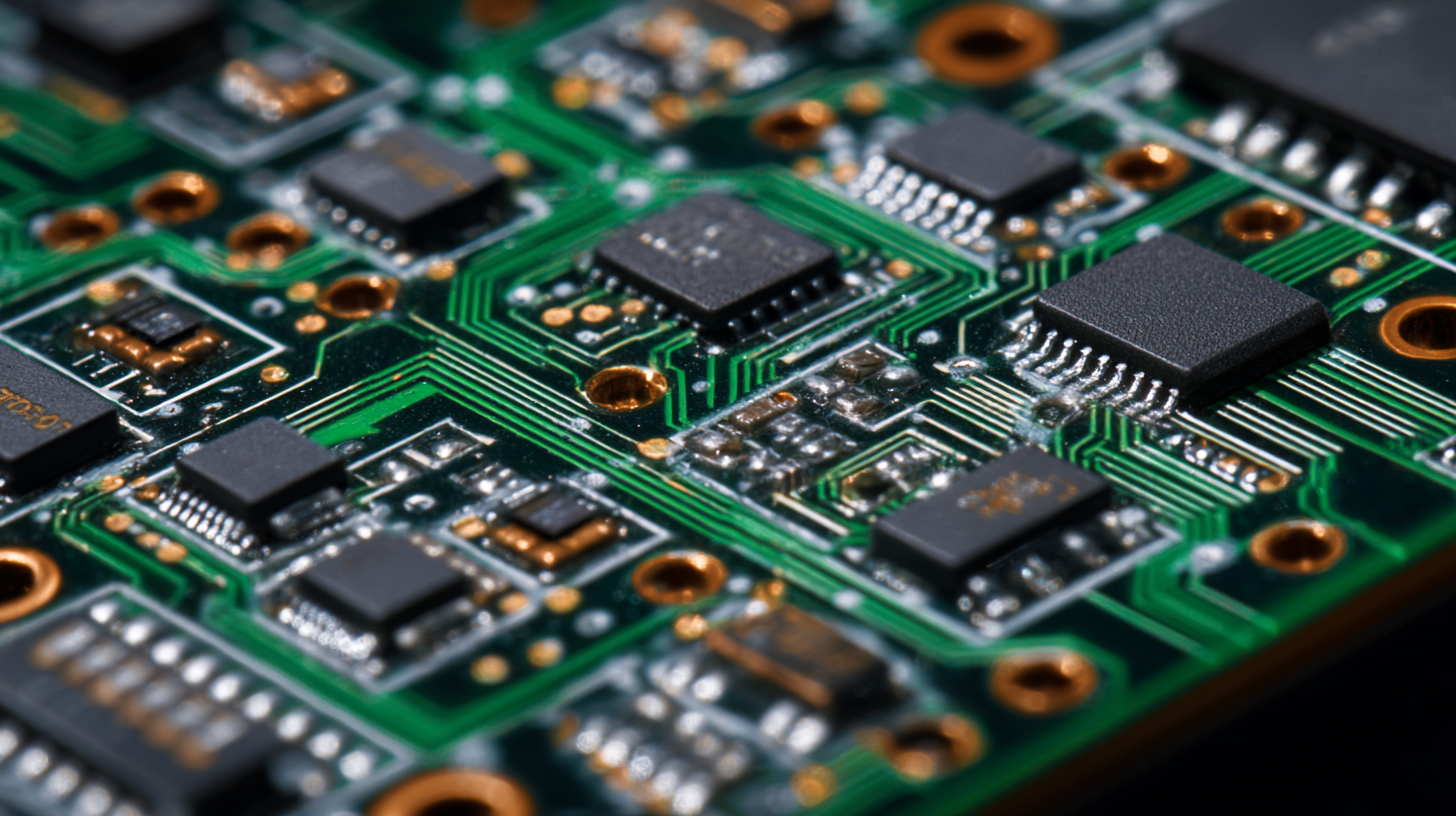
Optimizing Component Placement for Signal Integrity and Manufacturing Efficiency
When designing printed PCB boards, optimizing component placement is crucial for ensuring both signal integrity and manufacturing efficiency. One effective tip is to group components with related functions close to each other. This not only minimizes signal path lengths, reducing potential interference, but also simplifies the routing process, leading to a more streamlined workflow. Additionally, consider the thermal management of components. Placing heat-sensitive parts away from heat-generating components can significantly enhance the performance and longevity of the board.
Another important aspect is to prioritize the arrangement of high-frequency components. Positioning these parts towards the center of the board can help control impedance and minimize electromagnetic interference. This strategic placement, in combination with well-planned ground and power planes, supports more stable and reliable signals. Finally, maintaining a consistent grid layout for the components will aid in the manufacturing process, as it allows for easier automated assembly and testing, ultimately reducing production time and costs.
Utilizing Advanced CAD Tools to Streamline PCB Design Workflow
In today's fast-paced electronics market, utilizing advanced CAD tools to streamline PCB design workflow is crucial for achieving high-quality results efficiently. The global Engineering Software market, projected to grow significantly, underscores the increasing importance of integrated design solutions. By employing sophisticated CAD applications, designers can automate routing processes, which significantly reduces manual work and minimizes errors. This leads to faster prototyping and a more efficient path from concept to production.
Among the various available solutions, PCB design software integrates seamlessly with mechanical CAD systems, fostering better collaboration between electrical and mechanical engineers. This integration not only enhances communication but also ensures that design specifications are met across different disciplines. The use of advanced CAD tools thus not only improves the overall design quality but also accelerates the development cycle, allowing companies to respond more swiftly to market demands and technological advancements.
Incorporating Thermal Management Techniques for High-Performance PCB Design
Effective thermal management is crucial for enhancing the performance and reliability of printed circuit boards (PCBs). As electronic devices become increasingly compact and powerful, managing heat dissipation effectively has emerged as a fundamental component of high-performance PCB design. According to a report by IPC, nearly 40% of PCB failures are linked to thermal issues, underscoring the necessity for implementing robust thermal strategies during the design phase.
Incorporating techniques such as thermal vias, copper pours, and advanced heat sink solutions can significantly improve thermal performance. For instance, the use of thermal vias can facilitate heat transfer away from critical components, thus reducing local hotspots. A study conducted by the Electronics Cooling Journal highlighted that PCBs designed with proper thermal management techniques can sustain performance levels up to 20% higher than those without such measures. Furthermore, adopting materials with superior thermal conductivity, such as aluminum or polyimide substrates, can optimize thermal flow and improve overall system efficiency. As the demand for high-frequency and high-density electronic circuits continues to grow, engineers must prioritize thermal management to ensure their designs meet necessary operational benchmarks.
10 Essential Tips for Designing High-Quality Printed PCB Boards Efficiently
| Tip No. |
Design Tip |
Description |
Thermal Management Technique |
| 1 |
Layer Stack Optimization |
Select appropriate number of layers to minimize signal loss. |
Utilize core materials with better thermal conductivity. |
| 2 |
Via Placement |
Strategically place vias for optimal heat dissipation. |
Use thermal vias to connect heat-generating layers. |
| 3 |
Component Layout |
Group components to minimize trace lengths. |
Place heat-sensitive components away from heat sources. |
| 4 |
Trace Width Calculations |
Calculate trace widths based on current carrying capacity. |
Wider traces for high-current applications reduce heat. |
| 5 |
Solder Pad Design |
Ensure solder pads are adequately sized for components. |
Larger pads can improve thermal conductivity. |
| 6 |
Ground Plane Usage |
Utilize ground planes for better EMI performance. |
Ground planes also help in heat dissipation. |
| 7 |
Thermal Reliefs |
Incorporate thermal reliefs on pads connected to heat sources. |
Helps maintain lower thermal resistance to heat sinks. |
| 8 |
Simulation and Testing |
Simulate thermal behavior during design phase. |
Thermal simulations help identify hotspots early. |
| 9 |
Proper Material Selection |
Choose PCB substrates based on thermal properties. |
Materials with high thermal conductivity enhance heat flow. |
| 10 |
Monitoring and Feedback |
Implement methods to monitor thermal performance post-production. |
Feedback can guide future design improvements. |
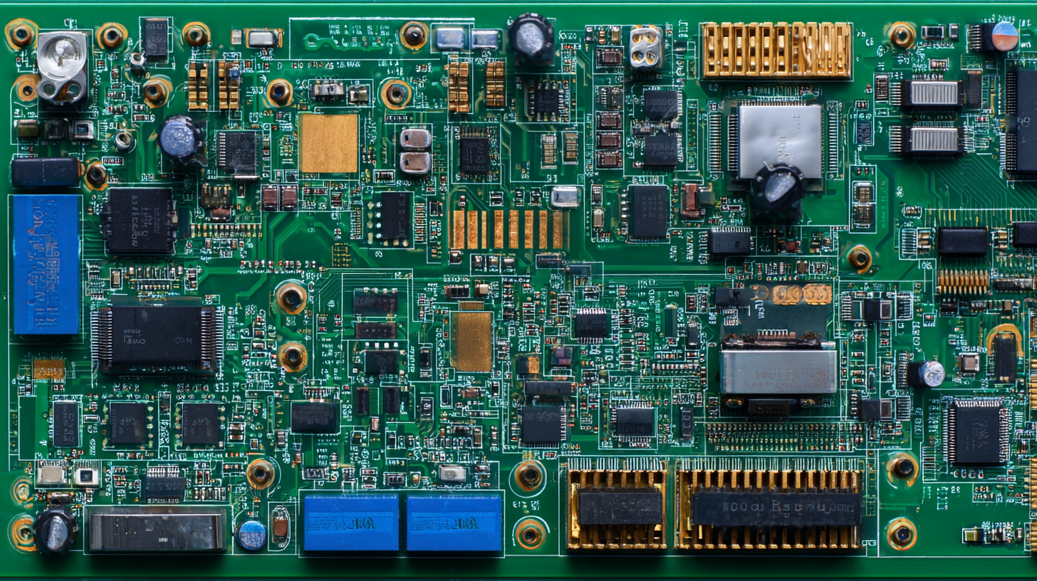
Exploring Manufacturing Tolerances and Best Practices for Reliable PCB Fabrication
When it comes to printed circuit board (PCB) fabrication, manufacturing tolerances play a crucial role in determining the quality and reliability of the final product. Recent industry reports indicate that tolerances for line width and spacing are narrowing, with a trend toward 3 mils or even less as technology advances. This precision is essential, as higher density designs are increasingly becoming the norm in modern electronics, requiring manufacturers to adhere strictly to these tolerances to avoid costly failures.
Furthermore, best practices for PCB design, such as incorporating appropriate component placement and optimizing routing techniques, significantly impact manufacturing efficiency. According to a 2022 report by IPC, a leading industry association, 65% of PCB defects stem from design-related issues. Implementing thorough Design for Manufacturability (DFM) strategies can mitigate these pitfalls. This includes using standardized components, minimizing trace angles, and ensuring adequate spacing between conductive paths to promote a smoother fabrication process. By focusing on these best practices and maintaining stringent manufacturing tolerances, engineers can enhance the overall reliability of PCB boards while optimizing production efficiency.