How to Design a Printed Circuit Board for Your Electronics Project?
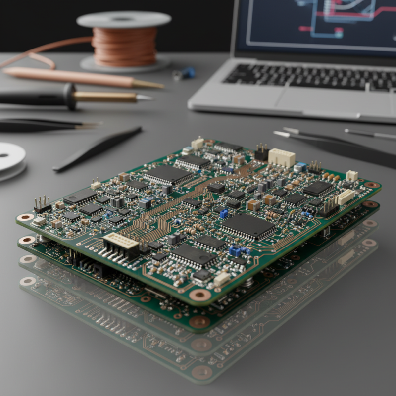
Designing a printed circuit board (PCB) is a vital step in any electronics project. A PCB is more than just a board; it serves as the backbone of your device. Proper design can enhance performance and reliability. However, it can be challenging for beginners. Mistakes can lead to malfunctioning circuits. Understanding the basics and nuances is essential.
Many factors impact PCB design. Component placement, trace width, and layout can influence functionality. Inefficient design can result in signal interference or overheating. A well-thought-out PCB can make a project successful. However, not every design will be perfect on the first try. Experimentation is often necessary to refine your approach.
Seeking expertise can help you improve your skills. Utilize online forums, tutorials, and software tools available today. Many resources provide guidelines and best practices for designing effective PCBs. Over time, you will gain confidence and capability. Learning from your design flaws is part of the journey. Embrace the process of creating a robust printed circuit board for your electronic endeavors.
Understanding the Fundamentals of Printed Circuit Board Design
Designing a printed circuit board (PCB) requires a solid grasp of fundamental concepts. Start with a clear schematic of your circuit. This visual guide lays the groundwork for your PCB layout. Use software tools to help translate your ideas into digital designs. Pay attention to component placement. Proper spacing prevents interference and ensures efficient routing.
Understanding signal flow is critical. Track power and ground lines wisely. Avoid long traces that can introduce noise. Thick traces can handle more current, but they also take up space. Reflect on your design choices. Sometimes, simple layouts are more effective than complex ones. Testing your design early can help identify issues.
As you design, think about manufacturability. Not all techniques are feasible for every project. Costs can climb with intricate designs. Balance performance and budget carefully. Accept that revisions may be necessary. Don't hesitate to iterate; each version brings you closer to a reliable PCB. Embrace the learning process. Mistakes can be valuable teachers.
How to Design a Printed Circuit Board for Your Electronics Project?
| Aspect |
Description |
Importance |
| Schematic Design |
Creating a circuit diagram that outlines the connections between components. |
Essential for visualizing and planning the board layout. |
| Component Selection |
Choosing appropriate components based on functionality and size. |
Crucial for ensuring the circuit meets the project requirements. |
| PCB Layout |
Arranging and routing components on the PCB. |
Important for space optimization and performance. |
| Design Rules Check (DRC) |
Verifying that the design adheres to manufacturing specifications. |
Critical for preventing errors that could cause manufacturing failures. |
| Gerber File Generation |
Exporting the design files used for manufacturing the PCB. |
Necessary for moving from design to production. |
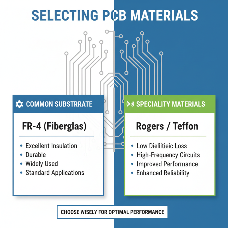
Selecting the Right Materials for Your PCB Project
When designing a printed circuit board (PCB) for your electronics project, choosing the right materials is crucial. The substrate material commonly used is FR-4. This fiberglass material provides excellent electrical insulation and durability. However, it may not be the best choice for every application. High-frequency circuits may benefit from materials like Rogers or Teflon, which have lower dielectric losses. Selecting the proper substrate can enhance performance and reliability.
Another critical consideration is copper weight. PCBs typically use standard weights of 1 oz or 2 oz per square foot. Thicker copper can handle higher currents, but it may also increase manufacturing costs. Think carefully about the current demands of your project. If you overlook this detail, you might end up with overheating issues that affect performance.
Additionally, consider the solder mask and silkscreen materials. The solder mask protects the board and prevents solder bridging. However, different colors and finishes can impact your project's aesthetic. Silkscreen is useful for labeling, but it can complicate the design. When making these choices, prioritize functionality over appearance. Revisiting and refining your choices during the design process is essential for a successful PCB.
Key Tools and Software for PCB Design and Simulation
Designing a printed circuit board (PCB) requires the right tools and software to ensure accuracy and functionality. The PCB design process is crucial for any electronics project. Current industry reports indicate that more than 70% of engineers use computer-aided design (CAD) tools for this purpose. These tools streamline the workflow and enhance precision in placements.
One vital software is PCB design applications that allow for layout creation and simulation. A study by the Institute of Electrical and Electronics Engineers (IEEE) suggests that incorporating simulation tools can reduce design errors by up to 30%. These tools enable designers to test their boards virtually before any physical prototype is made. This early identification of issues leads to better product quality.
However, the learning curve for these tools can be steep. Many users report frustrations in the initial stages of learning powerful software. Moreover, integrating different tools can complicate the workflow. Finding the right combination of software that fits an individual project’s needs often requires trial and error. It’s essential to remain adaptive and open to evolving design trends and technologies. This mindset allows for improvement and innovation in PCB design.
PCB Design Tools Usage Statistics
This chart illustrates the usage frequency of various PCB design tools among electronics project designers. As shown, Altium Designer is the most used tool, followed by Eagle, while CircuitMaker has the least usage among the listed tools.
Best Practices for Layout and Routing in PCB Design
When designing a printed circuit board (PCB), layout and routing are critical components. Effective placement of components can significantly reduce interference and improve performance. According to a report from IPC, improper layout accounts for over 30% of PCB failures. To mitigate these risks, consider the function of each component. Place high-frequency parts close together to minimize trace lengths.
Routing is another key aspect that demands attention. Aim for shorter traces to reduce inductance and capacitance. In fact, studies show that every inch of trace can increase the signal delay by 1.1 nanoseconds. Avoid sharp angles in traces; instead, use gentle curves or 45-degree angles for improved signal integrity. Layer stacking can also enhance your design, providing better separation for power and ground planes.
However, be aware of the trade-offs. Compact designs may struggle with heat dissipation. It’s crucial to leave enough space for heat sinks and air circulation. In some cases, a crowded layout might save space but lead to more troubleshooting later. Balancing density with reliability requires experience and careful planning. Consider iterative testing during the design process to identify potential flaws early.
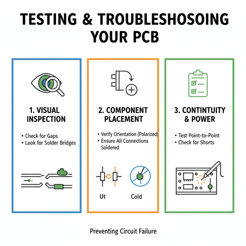
Testing and Troubleshooting Your Completed PCB Design
Testing a printed circuit board (PCB) begins with visual inspection. Look for gaps and solder bridges. A magnifying glass can help spot these issues. Verify component placement and ensure that all connections are soldered properly. Pay attention to component orientation, especially for polarized components. Errors in placement can lead to circuit failure.
Once the visual check is complete, power the board slowly. Use a multimeter to confirm voltage levels at various points. Check for shorts by measuring resistance across components. It’s common to overlook minor errors in the layout, which can cause malfunctions. If your board doesn’t perform as expected, retrace your steps. Review the schematic against the actual PCB design.
Test each section of the circuit individually. This can help isolate problematic areas. If an entire circuit fails, it may be due to a heat issue during soldering. Also, consider signal integrity. Noise can affect performance, often introduced through poor layout practices. Remember, each iteration of testing is a learning opportunity. Document issues and solutions to refine your design process.