How to Design and Manufacture Printed PCB Efficiently?
In the ever-evolving electronics industry, printed PCB is at the forefront. Research from IPC reveals that the global PCB market is expected to exceed $75 billion by 2025. This growth underscores the increasing demand for efficient design and manufacturing processes. Companies face challenges in keeping pace with this demand.
Efficiency in printed PCB production can significantly affect overall performance. Delays in design or manufacturing lead to lost opportunities and increased costs. A recent survey indicated that 30% of projects suffer from inefficiencies in PCB design. Factors such as complex layouts and material supply often contribute to these challenges.
Moreover, sustainability issues are becoming critical. The need for eco-friendly materials is rising. Consumers are seeking more responsible production practices. Companies failing to adapt may find themselves at a disadvantage in the market. As the industry grows, reflections on improving current practices are essential.

Understanding the Basics of Printed Circuit Board (PCB) Design
Understanding the basics of printed circuit board (PCB) design is crucial for efficient manufacturing. A well-designed PCB minimizes material waste and optimizes production time. In fact, industry reports show that around 30% of manufacturing costs are directly linked to poor PCB design. Thus, investing time in the design phase is essential.
Effective PCB design considers factors such as layout, layer count, and materials. For instance, utilizing a multi-layer design can increase complexity but improve performance. Unfortunately, many designers overlook the significance of a thorough design review. Studies indicate that flawed layouts can lead to rework rates as high as 25%. This can significantly delay project timelines and inflate costs.
Another important aspect is the selection of materials. Using high-quality substrates can enhance the PCB's reliability. However, premium materials often come with a higher price tag. Balancing quality with cost is a challenge many face. Many designers find themselves stuck in the cycle of cutting corners to save money, only to face issues later on. Assessing priorities and learning from each project will help in making more informed decisions in the future.
PCB Manufacturing Process Efficiency
This bar chart illustrates the time allocation for each phase in the PCB manufacturing process. Understanding these phases helps in optimizing the overall efficiency of PCB design and production.
Key Considerations in PCB Layout and Design for Efficiency
Designing an efficient printed circuit board (PCB) involves careful consideration of layout and design elements. Harmony between components is crucial. Gaps should be minimal, yet allow for heat dissipation. Think about the placement of power and ground planes. They should provide a clear path for electrical signals while reducing interference.
Using the right design tools makes a significant difference. Many designers overlook the importance of simulation software. It can predict potential issues before manufacturing. However, some tools may lack user-friendly interfaces, causing designers to hesitate. Don’t rely solely on automated systems. Manual checks can catch mistakes that software might miss.
Thermal management is often neglected in the early design stages. Heat can damage components over time. This requires a strategic layout and an understanding of how heat spreads. It may not seem urgent, but in the long run, it’s a critical factor. Reflection on these details may lead to a more efficient PCB design. Small changes in layout can yield significant efficiency gains. Design is a journey, not a destination. Each iteration brings lessons learned and areas for improvement.
Selecting Appropriate Materials for PCB Manufacturing
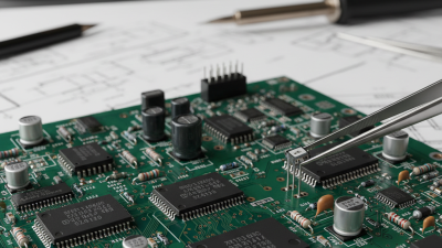
Selecting the right materials for PCB manufacturing is crucial. High-quality materials ensure durability and functionality. The choice of substrate is especially important. FR-4 is popular, but alternatives like polyimide can offer better thermal performance. Think about your project's specific needs.
Conductivity matters too. Copper is commonly used for traces, but the thickness can vary. Thicker copper can handle higher currents but may increase costs. Keep in mind, too thick a copper layer might complicate the manufacturing process.
Another consideration is the type of solder mask. While options like green solder mask are common, other colors can affect heat dissipation. This choice might seem minor but can impact performance. Reflecting on material selections helps you avoid future issues. Always evaluate trade-offs in quality, cost, and performance. Mistakes in this area can lead to bigger headaches down the line.
How to Design and Manufacture Printed PCB Efficiently? - Selecting Appropriate Materials for PCB Manufacturing
| Material Type |
Properties |
Applications |
Cost per Square Foot |
| FR-4 |
Good electrical insulation, flame retardant |
General electronics, consumer products |
$5 - $10 |
| CEM-1 |
Lower thermal resistance, good machinability |
Single-sided PCBs, low-cost applications |
$4 - $8 |
| Polyimide |
Excellent thermal stability, chemical resistance |
Aerospace, high-temperature applications |
$20 - $30 |
| Rogers Material |
Low dielectric loss, high-frequency performance |
RF applications, antennas |
$40 - $60 |
Streamlining the PCB Production Process: Techniques and Tools
In the fast-paced world of electronics, efficiency is key. Streamlining the PCB production process can greatly enhance workflow. One effective technique is to use software tools that automate design checks. These tools catch errors early and save time in later stages. Designing in layers, with clear markings, helps avoid confusion during manufacturing. Each layer should have a consistent structure, ensuring better alignment.
Collaboration is also vital. Teams should communicate about design goals to avoid rework. Regular meetings can help track the project’s progress. Utilizing rapid prototyping can minimize lead time. It allows for immediate adjustments based on testing. This step is crucial, as it often reveals design flaws that require attention.
However, not all techniques will fit every project. Rigid adherence to a single process can lead to constraints. It’s important to remain flexible and adapt based on project needs. Reflection on previous projects can inform better decisions. Each attempt may not yield perfection, but they offer invaluable insights for future designs. Emphasizing improvement can lead to more efficient PCB production overall.
Quality Control and Testing Methods for Efficient PCB Manufacturing
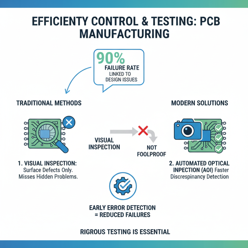
Quality control and testing are vital in PCB manufacturing. With around 90% of PCB failures linked to design issues, rigorous testing is necessary. Visual inspections help identify surface defects. However, this process can miss hidden problems. Implementing automated optical inspection (AOI) systems can catch errors early. AOI detects discrepancies faster than manual methods, but it isn’t foolproof.
Functional tests, like in-circuit testing (ICT), check for electrical errors. Studies show that ICT can increase fault detection rates by 95%. Yet, these tests require skilled technicians to interpret results. The margin for human error remains a concern. Some manufacturers overlook the importance of training, which can lead to mishandling issues.
Environmental testing measures PCB performance under different conditions. Thermal cycling and humidity tests expose weaknesses. But, the cost of extensive environmental testing can be prohibitive. Many companies underestimate this expense, risking future failures. Developing a balanced approach to testing and quality control is critical. Relying solely on one method may not catch all potential problems, necessitating a more holistic strategy.