Let Us Know How We Can Help. We Are Your Dedicated Solutions Provider.
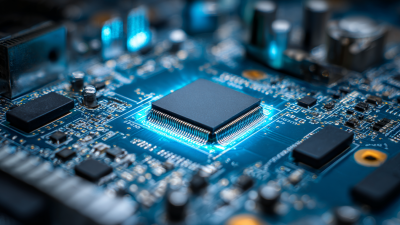
Designing a PC board can be a challenging but rewarding endeavor. The process requires careful planning and attention to detail. A well-designed PC board forms the backbone of your electronic projects, affecting functionality and performance.
When creating a PC board, understanding its layout is critical. Each component has its place and must be positioned correctly. Mistakes in spacing can lead to failures. You may need to revisit your design several times to refine it. This iterative approach is part of learning.
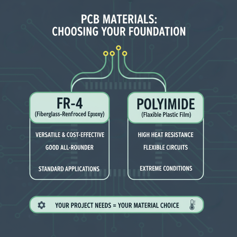
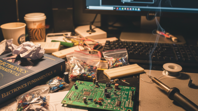
Lastly, consider the materials you use. Different boards have varying levels of durability and conductivity. Sometimes, choices can lead to unexpected results. Reflection on these decisions can guide your future designs. Embrace the learning curve as you craft your ideal PC board.
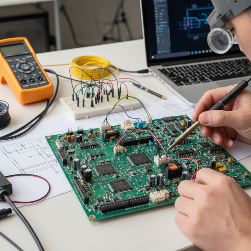
Designing a PCB board requires a solid understanding of the basics. Start by determining your project's needs. What components will you use? Consider size, layout, and how parts connect. Each decision affects the board's functionality.
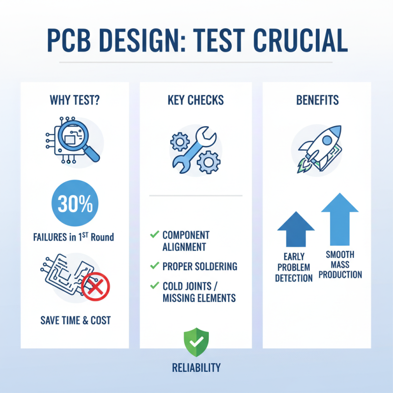
When sketching your design, pay attention to the flow of electricity. Traces should be clear, avoiding unnecessary bends. However, mistakes often happen. Rushing can lead to shorts or open circuits. It’s crucial to review the diagram multiple times. Take breaks; fresh eyes may catch errors you missed earlier.
After designing, select appropriate materials. Choose a substrate with the right thickness. This choice impacts durability and performance. Remember, no design is perfect. Testing your board may reveal flaws. Use this feedback to refine your next project. Learning from each design helps you grow as a maker.
Selecting the right materials for your PCB is essential. The substrate is the backbone. It affects durability and performance. Common choices include FR-4 and polyimide. FR-4 is versatile and cost-effective. Polyimide offers higher heat resistance. Choose based on your project needs.
Tips: Consider the environment. Will the PCB face humidity or extreme temperatures? Use materials that withstand those conditions. Think about the application. Is flexibility required? Use flexible PCB materials in such cases.
Copper thickness matters. Thicker copper can handle more current. But it also adds weight and cost. A balance is key. Evaluate the power requirements of your design. Sometimes, a thinner option suffices.
Don't overlook the soldermask. It protects the copper and reduces short circuits. Different colors are available, but the function is consistent. Choose the right color for visibility or aesthetic reasons. Reflect on your design goals. Choosing materials is not just technical; it shapes your project’s success.
Creating schematic diagrams is a crucial step in designing a printed circuit board (PCB). A schematic diagram visually represents circuit components and their connections. It helps you understand how the circuit works. Using software tools, you can start placing components, such as resistors and capacitors. Always check their connections carefully. A small mistake can lead to significant issues.
Start with a basic layout. Arrange the components logically. Keep similar parts close together. This simplifies the connections later. Use clear labels for each component. Readability is essential. If your diagram is cluttered, it can confuse you during the assembly process. Review your work frequently. This can reveal potential errors before they become a problem.
Don’t hesitate to seek feedback from peers. They may spot mistakes you’ve missed. It's a learning experience, and every iteration improves your design. Be prepared for revisions. Your first draft may not be perfect. Embrace the challenges, as they are part of the process. An effective schematic can greatly ease the PCB design phase of your projects.
| Component | Type | Value | Footprint | Notes |
|---|---|---|---|---|
| Resistor | Passive | 1kΩ | 0402 | Standard value for pull-up |
| Capacitor | Passive | 10µF | 0603 | Decoupling capacitor |
| Microcontroller | Active | ATmega328 | TQFP-32 | Popular for DIY projects |
| LED | Active | Red | 0402 | Indicates power status |
| Transistor | Active | 2N2222 | TO-92 | General-purpose NPN transistor |
Designing a PCB can be thrilling yet challenging. When laying out your circuit board, there are key techniques to consider. Start by organizing your components logically. Group them based on function, like power and signal. This reduces noise and interference.
Keep traces short and direct. It minimizes resistance and inductance.
Pay attention to trace width. Wider traces can handle more current. You might make mistakes here. Too narrow, and you risk overheating. Don't forget about grounding. A solid ground plane is essential for stable performance. You might notice issues if it’s poorly designed.
Layout tools can help visualize connections. Yet, they may not catch every mistake. Always double-check your work.
Lastly, consider the manufacturing process. It can influence your design choices. Sometimes, a well-intentioned layout may not be manufacturable. This can lead to frustration and delays. Prototyping is crucial. Testing your design helps find hidden flaws. Remember, each iteration improves your skills and knowledge.
Testing your finished PCB design is crucial. It helps identify issues before mass production. According to a recent industry report, about 30% of PCB designs encounter problems in the first round of testing. Identifying these issues early can save time and costs. Ensure all components are properly aligned and soldered. Inspect for potential cold joints or misplaced elements.
A common mistake is overlooking power integrity. Use an oscilloscope to measure voltage at various points. A discrepancy can signal design errors. If signals are inconsistent, analyze your traces. Their length and routing can impact performance significantly. Additionally, employing a thermal camera helps identify overheating components, which might indicate a design flaw.
Include a revision plan based on your tests. Document every failure encountered during testing. This data can guide improvements for future designs. Adjustments may include altering trace widths or adjusting component placements. Don’t shy away from revisiting your design based on findings. This iterative process sharpens your skills and enhances future projects.