Let Us Know How We Can Help. We Are Your Dedicated Solutions Provider.
PCB board design is essential for creating efficient electronic devices. As technology advances, the complexity of designs increases. This makes it crucial for both beginners and professionals to grasp the fundamental principles of PCB board design.
In this guide, we will explore valuable tips tailored for various skill levels. Understanding layout techniques, component placement, and signal integrity can drastically improve your designs. However, even experienced designers may overlook minor details. These oversights can lead to circuit failures or design inefficiencies.
Practicing a thoughtful and methodical approach in PCB board design is key. Learning from mistakes will enhance your skills. Every project presents unique challenges. Embracing these challenges will ultimately lead to better designs and improved understanding of the process.
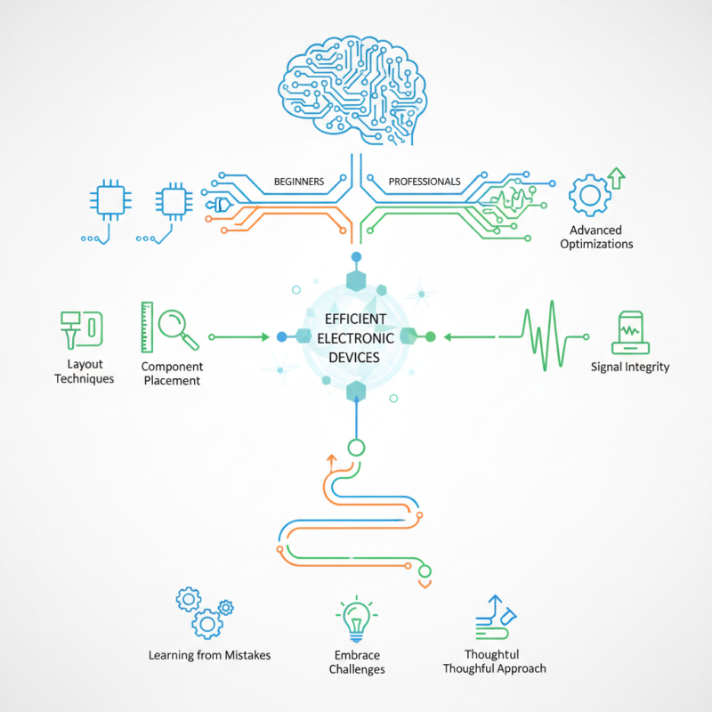
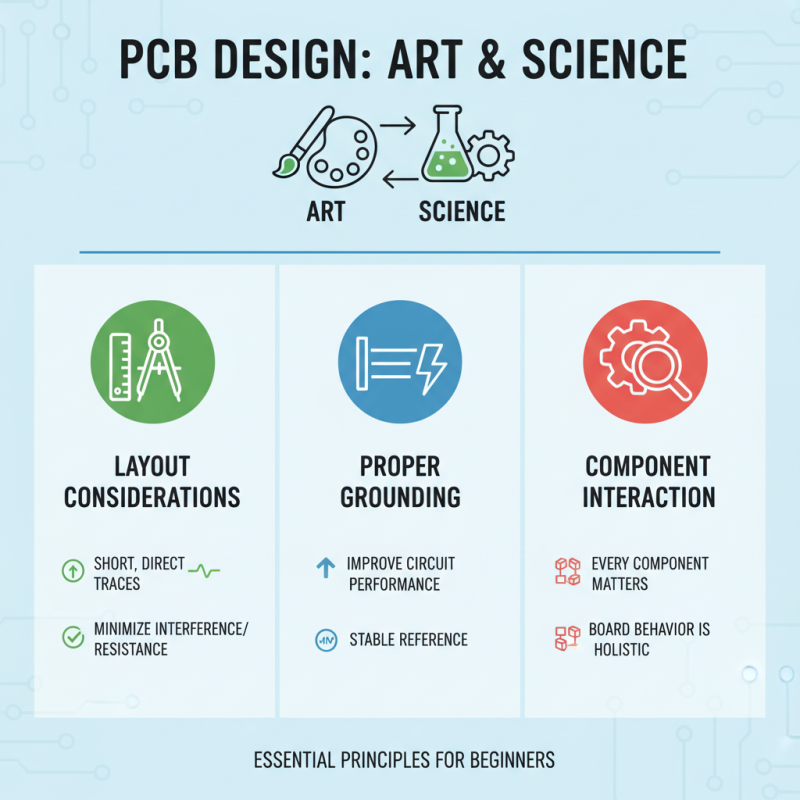
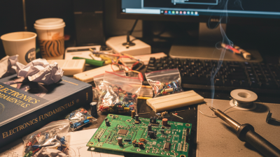
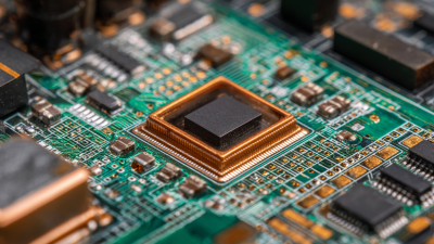
PCB design is both an art and a science. Understanding the essential principles is crucial for anyone entering the field. Start with layout considerations. Keep traces short and direct. This minimizes resistance and potential interference. Using proper grounding techniques can drastically improve circuit performance. Remember, every component affects the overall behavior of the board.
Next, component placement matters. Group related components together. This reduces the length of connections and enhances signal integrity. Avoid placing sensitive components near noisy ones. Trial and error is part of learning. Mistakes in placement can lead to malfunctioning circuits. Analyze and reflect on these errors for future designs. A well-thought-out design can save time and resources in the long run.
In PCB design, selecting the right software tools is critical for creating effective layouts. A report from IPC estimates that over 80% of defects arise from poor design practices. To reduce these issues, using intuitive design software can make a significant difference. Many tools today offer real-time simulation capabilities. This allows designers to visualize how their boards will perform, minimizing costly iterations.
When choosing PCB software, consider the ease of use. Many beginners struggle with complex interfaces, which can stall progress. Opt for tools that offer drag-and-drop functionality. Simplicity can lead to faster designs. Additionally, incorporating simulation features from the start can help you spot issues early.
Another tip is to invest time in learning the software’s features. Users often underutilize available tools, missing out on automated checks that could catch mistakes before fabrication. Emphasizing this learning curve is vital for both new and experienced designers. After all, a missed design rule could lead to failures, costing time and resources. Prioritizing education on these tools can enhance the overall design process.
When designing printed circuit boards (PCBs), schematic design and component placement are critical elements. Effective schematic design reduces errors. Research indicates that over 40% of design issues stem from poor schematics. Clear connections and logical layouts promote better understanding among team members. Keeping the design straightforward also minimizes the time required for troubleshooting later in the process.
Component placement requires attention to detail. Place components compactly to reduce trace lengths. This can significantly improve signal integrity and reduce noise. However, it’s essential not to prioritize size over functionality. Components in close proximity can heat up, leading to potential failures. A good rule of thumb is to leave some space around heat-sensitive components. Reports show that around 30% of PCB failures are heat-related. Designers should also anticipate manufacturing constraints. Certain placements may complicate the production process, leading to delays or increased costs.
Consistent practices are vital in both schematic design and component placement. Documentation is often overlooked but can bridge communication gaps within teams. Lack of documentation has been linked to a rising number of design revisions. Even experienced designers can benefit from establishing clear guidelines. Reflecting on past projects can help identify common pitfalls, making future designs smoother and more efficient.
| Design Aspect | Best Practices | Common Mistakes |
|---|---|---|
| Schematic Design | Ensure clear labeling of all components and connection lines. | Neglecting to keep track of component values and connections. |
| Component Placement | Place components logically and ensure minimal trace lengths. | Crowding components and ignoring thermal management. |
| Trace Routing | Use wide traces for high current paths and avoid sharp corners. | Overlooking the impedance of traces and using narrow traces. |
| Power Distribution | Design an adequate ground plane and separate analog/digital grounds. | Ignoring the importance of a solid ground reference. |
| DFM Considerations | Design for manufacturability by following fabrication guidelines. | Failing to account for the tolerances of the manufacturing process. |
Effective route optimization is essential for PCB design. Good routing minimizes signal integrity issues. Short, direct paths reduce delays and interference. Each trace on the board influences performance. Strive for symmetry in trace lengths. It helps maintain balanced signals. Avoid sharp angles. They can cause signal reflection and degradation.
Signal integrity management is another key consideration. Use proper grounding techniques to ensure stable reference points. Keep power and ground traces wide and short for better performance. Separate signal lines from noisy power traces. This can help prevent crosstalk. Pay attention to the dielectric material as well. Different materials affect impedance and signal speed.
Be aware of your mistakes. You might overlook some components during layout. Regularly reviewing your design will catch potential issues. Use prototypes to test your designs. Learning from failures is a significant part of growth in PCB design. Embrace the iterative process, and keep refining your approach.
In PCB design, avoiding common mistakes can make or break a project. Many beginners overlook the importance of proper component placement. Every component should be easy to access and test. Dense layouts often create heat issues. Heat management is crucial for performance. Prioritize airflow.
Another frequent mistake is ignoring the ground plane. A solid ground plane minimizes noise and ensures stable performance. Inadequate grounding often leads to signal integrity issues. Pay attention to trace widths as well. Too narrow traces can cause overheating. It’s wise to use a PCB calculator to determine the appropriate widths.
Beginners may also forget to double-check their footprints. An incorrect footprint can render a design unusable. This mistake is usually hard to detect until assembly. It’s beneficial to take time for design checks. Design reviews can highlight overlooked details. Rushing through the design can lead to regret later. Reflecting on these aspects can elevate your skills significantly.